This judgment was handed down remotely at 10.30am on 31 July 2024 by circulation to the parties or their representatives by e-mail and by release to the National Archives.
- The rapid development of integrated circuit chips since their invention in 1959 has sometimes created technical difficulties not found in early versions of the technology. One such has been the generation of higher voltage spikes in the chip as a consequence of progressive miniaturization and increased efficiency. If severe, the spikes can damage the chip so that it ceases to function. Even if less severe, the functional life of the chip is liable to be reduced. The Claimant ("R2") says that it recognised the problem early and devised a solution which led to the grant of its European Patent No. 3 376 653.
- R2 alleges that the Defendants (collectively "Intel") have infringed the UK designation ("the Patent") by marketing chips, processors and other microelectronic devices containing certain fully integrated voltage regulators, or FIVRs. "Fully integrated" means that the regulator is a component of the chip itself as opposed to being an external item connected to the chip. R2 says that these FIVRs prevent voltage spikes in Intel's chips in accordance with the invention and are products falling within the claims of the Patent.
- Intel have counterclaimed, alleging that the invention lacks novelty or inventive step over a single cited item of prior art and that the Patent is also invalid on the grounds of added matter and insufficiency.
- R2 has made a conditional application to amend the claims in either of two alternative ways.
- Brian Nicholson KC, Adam Gamsa and Edmund Eustace appeared for R2, Andrew Lykiardopoulos KC and Anna Edwards-Stuart KC for Intel.
The witnesses
- R2 instructed two expert witnesses. One was Professor Eduard Alarcón who is Professor of Electrical Engineering at the Technical University of Catalunya. He gave evidence principally about the common general knowledge of the skilled person, terms used in the Patent and issues arising on validity. The other was Dr Selçuk Köse, Associate Professor of Electrical and Computer Engineering at the University of Rochester, New York State. Dr Köse gave evidence about the computer models used by the parties from which figures were derived relating to the issues on infringement, including the computer models used by R2 in their experiments.
- Intel had one expert, Professor Bram Nauta, head of the Integrated Circuit Design Group at the University of Twente in the Netherlands. In addition Intel had a witness of fact, Christopher Schaef. Dr Schaef's witness statement explained the computer models used by Intel in their experiments on infringement. Until March 2024 Dr Schaef was an employee of a company in the Intel group.
- All four were very good witnesses, giving clear and helpful evidence.
The technology
- The content of this section was all part of the skilled person's common general knowledge (CGK) at the priority date. It is not exhaustive; other matters within the CGK will be discussed in the context of the issues in the case.
Printed circuit boards and integrated circuits
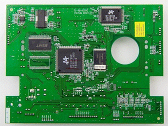
- Electrical devices such as computers and mobile phones function by means of a multitude of circuits which connect components such as inductors, capacitors, resistors and transistors. These components may exist as discrete items or may be incorporated into what are called "integrated circuits" (ICs) or "chips". The discrete components and ICs are mounted on a printed circuit board (PCB) and are connected to each other by wires or metal traces. This is a plan view of a PCB:

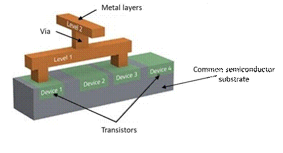
- ICs have a substrate base of semiconductor material supporting the components of the IC which are connected by metal deposited above the components in one or .more layers. This diagram illustrates the basic structure of an IC with the components marked "devices", two of them (arbitrarily) shown as transistors and two layers of metal connecting the components, the metal layers being connected by a "via":

Resistors, capacitors and inductors
- A resistor resists the flow of current passing through it. Resistance is measured in Ohms (Ω). A capacitor stores charge; the unit of capacitance is the Farad (F). Inductance is the tendency to oppose change in the flow of current, measured in Henrys (H).
- These electrical phenomena are not exhibited only by individual resistors, capacitors and inductors. Any part of a circuit has a combined resistance, capacitance and inductance, governed by its component parts.
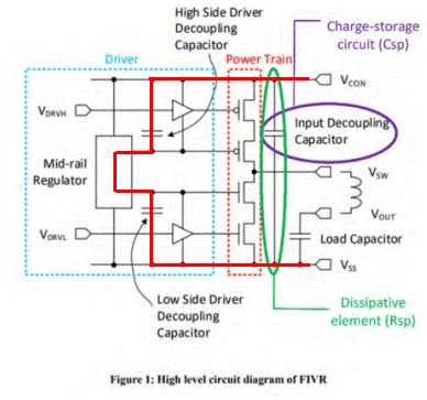
- A type of capacitor known as a "MIM capacitor" is used in the accused Intel FIVRs. MIM denotes the metal-insulator-metal construction of a capacitor, to be distinguished from metal-oxide-metal (MOM) and metal-oxide-semiconductor (MOS) capacitors.
Transistors
- Transistors are core devices of all ICs. The following is a description of a type of transistor relevant to this case, known as a "field-effect transistor" (FET). A FET is a device with three terminals through which the transistor is connected into a circuit. The three terminals are called the gate, the source and the drain terminals. The source and drain terminals are separated by a region called the channel. The operating principle of a FET is that by applying a voltage to the gate terminal the conductivity of the channel between the source and drain can be controlled. Accordingly, the voltage applied at the gate is used to control whether a conductive channel is created, if so how conductive it is, and therefore how much current is permitted to flow between the source and drain terminals.
- A transistor can be operated like a switch, allowing current to flow through the channel between the source and drain when a certain minimum voltage is applied to the gate terminal, but fully or partially blocking the flow of current when a lower voltage is applied. When a transistor is in its "off-state", the resistance of the channel is high, preventing the flow of current. In the "on-state" reduced resistance in the channel means that current will flow relatively freely between the source and drain terminals. Between those two states there are intermediate levels of resistance so that current flows at a reduced rate.
Power converters and regulators
- A functioning circuit is powered by a source of electrical current. "Power converter" is an umbrella term which describes circuitry which alters the power provided at the input of the circuitry to power with different properties at the output. The conversion could be to change the shape of the waveform of the current, for example by converting AC to DC, or by changing the frequency of the waveform. Another possibility is that the output voltage is changed relative to the input voltage while preserving the power level.
- Power converters use combinations of active switching devices, such as transistors, circuitry to control the operation of the active devices (control circuitry) and reactive (passive) components such as capacitors and inductors to perform the desired conversion.
- Voltage regulators are a subset of power converters that convert one DC voltage to another DC voltage and are designed to provide a regulated output (although "voltage regulator" and "power converter" were often used interchangeably in the evidence). The output of a voltage regulator should be a stable DC current with a fixed desired voltage irrespective of changes in voltage supply and current demand, subject always to the limitations of the regulator.
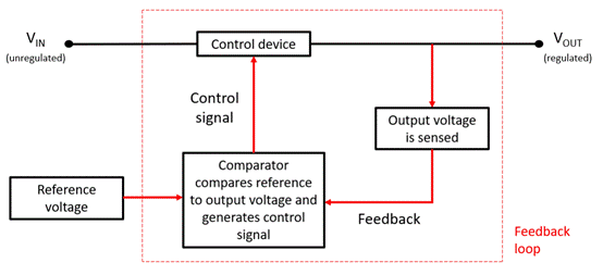
- Voltage regulation is typically achieved by the use of a feedback loop through the control circuitry. The feedback loop senses information, generally the voltage at the output of the regulator circuitry, and uses this to change the way in which the active devices operate. This can be shown diagrammatically:

Decoupling capacitors
- Capacitors are often used at the input of a voltage regulator. These are known as "decoupling capacitors". Their purpose is to separate, or decouple, the voltage regulator from other parts of the power management circuitry. Decoupling capacitors act as a charge reservoir to supply charge to the input of the voltage regulator when the input voltage drops below the desired level and to reduce input voltage variations.
Linear and switching regulators
- A linear regulator takes the form of a variable resistance placed in series or parallel with the load to be powered. A control circuit adjusts the resistance to ensure that the voltage at the output of the regulator is constant.
- Linear regulators are to be distinguished from "switched mode" or "switching regulators", with which the Patent is concerned. These achieve the same result by more complex means. A DC current applied at the input of the regulator is switched on and off. Components such as inductors and capacitors, governed by a control circuit in combination, convert the time varying signal to a DC current with a fixed voltage different from the input voltage. The principal advantages of switching regulators are that they can increase the voltage, not just reduce it and in many applications they are much more efficient. In the case of battery-powered devices, the improvement in efficiency is especially of value, significantly enhancing battery life.
- Most switching regulators must have physically large inductors and capacitors to perform their function in keeping the variation or "ripple" in the current fed to the load to a minimum.
Buck converters
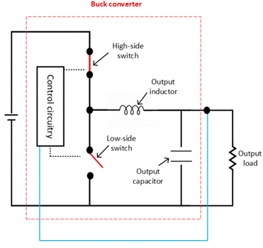
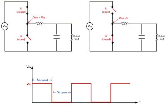
- A buck converter is a switching regulator which steps down the supply voltage to a lower DC voltage. It typically contains two switching devices, commonly transistors, one at the "high side" i.e. at the point of input of the current, and one at the "low side" towards the output. There is control circuitry including a feedback loop to control the operation of the switching devices and an inductor and capacitor at the output of the node between the two switching devices, called the "common node" or the "switching node". This is a diagram of a buck converter:

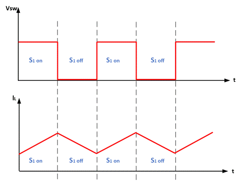
- The sequential opening and closing of the two switching devices results in a square waveform of voltage measured over time at the switching node. This can be illustrated as follows:

- This variation in current, in square waveform, passing through the inductor, causes the current in the inductor to rise and fall in a triangular waveform, called inductor current "ripple", shown here:

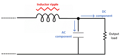
- The inductor current ripple is made up of an AC and DC component. At the output of the inductor in the buck converter a capacitor is connected in parallel with the load. This filters out the AC component of the inductor current ripple, leaving only a DC current to be passed to the load. The capacitor provides a low impedance path for the AC part of the inductor current but blocks the DC component thereby allowing the DC to pass in the direction of the output load. This results in the AC component of the inductor current passing through the capacitor branch of the parallel circuit, leaving the DC component to pass through the other parallel branch of the circuit and on to the load:

- Ideally, the output voltage of a buck converter will contain no AC component at all but in practice there is a residual AC component known as the "output ripple". Output filter components, an inductor and a capacitor, can be used to minimise the ripple. A more sophisticated technique to deal with output ripple is called "interleaving", which is possible where the buck converter produces current in two phases. I will discuss this below.
CMOS transistors
- A variety of FET transistor is a metal oxide semiconductor FET, or MOSFET. A process has been developed in which MOSFET transistors are configured so that a gate voltage which turns on one transistor turns off the other. Such pairs of transistors are called CMOS transistors. They have become the predominant transistors in IC technology because they allow for a compact arrangement of components and require very low gate voltages, meaning that power consumption is reduced.
The skilled person
- The skilled person may be a team. The person or team has experience in integrated circuit design, power electronics and the design of voltage regulators. They will have knowledge of on-chip power management and voltage regulators. The parties were agreed on this. R2 thought that the relevant qualities would be possessed by an individual, Intel favoured a team. I will speak of the skilled person but it makes no difference.
- A point was made by R2 about the distinction between a designer of digital components of a circuit and a designer of analogue or mixed signal components. The evidence did not in the end establish that the distinction, such as it is, would have made a material difference to the perspective of the skilled person in this case.
The Patent
- The Patent is entitled "Over voltage protection of a switching converter". It has an unchallenged priority date of 23 December 2009.
- The description begins with a general discussion of voltage regulators, noting that the Patent is concerned only with switched regulators ("switched" and "switching" are used interchangeably).
- The switching frequency of a regulator is the rate at which the switching device in the regulator alternates between on and off. The Patent explains that the higher the switching frequency, the smaller are the sizes of inductor and capacitor necessary to perform their function. This allows the use of planar shaped inductors which can be accommodated on PCBs or fabricated in integrated circuits.
- The Patent identifies a downside to high frequency switching. It generates two types of energy loss which must be kept to a minimum if the converter is to be adequately efficient.
- The first is transition loss, which occurs when the current flow is transitioning between zero, when the switch is open, and maximum current when the switch is closed. The same applies to the transition from maximum current to zero when the switch opens. The time taken to make the transition in each case (the Patent assumes they are the same) is the "switching time".
- The second energy loss is gate charge loss: the voltage at the gate of the transistor must be charged to change its state from open to closed or vice versa. The charging energy is usually lost.
- Prior art means of minimising both types of loss and the disadvantages of those solutions are set out.
- The Patent goes on to describe the advantages of the very fast switching times characteristic of advanced transistors. Because these transistors are in the transition state (zero to maximum current and the reverse) for very short periods, transition loss is minimised. In addition, the voltages required to implement a gate change are lower in advanced transistors, so gate charge loss is also reduced.
- The switching time is to be distinguished from the frequency of switching. It is possible to have high frequency switching but relatively soft, or slow, switching times.
- Advanced transistors have short channel lengths and thin oxides. Although it is this which permits a lower gate switching voltage, it also means that the maximum voltage which the transistors are able to tolerate is lower. The Patent states that a conventional buck converter circuit will therefore not operate reliably. It continues:
"[0022] Therefore, there exists a need for a DC-DC converter that is simultaneously compact (including optimally fabrication of all active and passive components on a single semiconductor die), low in cost, and highly efficient even at small ratios of output to supply voltage and low output current.
[0023] It is desirable to have a method and apparatus for protecting switching elements of a converter from transient voltages to allow fast low-loss switching operations without degradation of reliability."
- In a further passage providing details of how such a converter may be made, the Patent emphasises the need to avoid (a) excessive voltage stress to the switching transistor and (b) excessive voltage appearing between any two transistor terminals.
- In a section headed "Spike Protection Circuit" the Patent states that there will be parasitic inductance associated with the connection between the battery, or other external power supply, and the high-side switch.
- Parasitic inductance is generally unwanted inductance which is inherent in any electrical circuit, both as a whole and in its component parts. Similarly, there is always parasitic resistance and parasitic capacitance. A high-side switch is a switch upstream of the load. It turns the current applied to the load on and off. When the switch is a switching transistor and is turned off, the parasitic inductance will resist the sudden change of current and a voltage spike will be generated.
- The Patent continues: voltage spikes associated with very fast switching transitions are liable to exceed the maximum tolerated by the transistor. Also, the parasitic inductance will interact with parasitic capacitance to form a high-frequency resonant circuit which will create persistent "ringing". Ringing is an oscillation or ripple in voltage or current output.
- The Patent states that spike protection circuitry is required in the form of charge-storage circuits comprising capacitive elements. In addition, dissipative impedance is desirable to dissipate the ringing:
"[0067] It should be noted that voltage spikes will occur in any converter that has fast switching transitions without added shunt capacitance around the switches, irrespective of whether the switching elements are stacked NMOS switches, or any other type of switch that includes, for example, PMOS transistors, a single PMOS transistor, a single NMOS transistor, or any other fast switching device. Additionally, while the detailed behavior shown in Figure 18 may be specific to the described embodiments, the general phenomena of excessive voltage excursions (spikes) and ringing will occur any time a fast switching transition without added shunt capacitance is used in a converter."
- Thus, the advantage of using advanced transistors with fast switching times also carries the disadvantage that voltage spikes and ringing will be generated, which will require shunt capacitance to deal with them. The specification does not say that this is new information, although at [0065] the reader is told that the problem has been typically neglected, either because low frequency converters were used or because the high frequency converters used had relatively slow switching times.
- The point of the invention is then identified:
"[0068] Clearly, it is desirable to provide spike protection circuitry for the series and shunt switch elements of any DC-DC converter employing fast switching transitions as described above. Ideally, the spike protection includes capacitive elements between previously described first voltage supply and second voltage supply. For an embodiment, the spike protection circuitry includes a transmission line having minimal parasitic inductances, thereby minimizing the impedance of the transmission line."
- The Patent points out that capacitance sufficient to protect the transistors from voltage spikes will lead to an increase in the physical size of the capacitor and this creates increased parasitic inductance. A solution is explained (here omitting reference numbers):
"[0078] A solution to this problem can be found by further subdividing switching elements of the switching circuitry into segments (switching block segments) connected in parallel, such that each segment carries a portion of the total output current, and further partitioning the protection circuit Csp - Rsp into separate segments, each protecting one of the switching block segments."
- In other words, the current is divided between blocks of switching transistors, so that the exposure of each block to voltage spikes is reduced, with the protection circuitry correspondingly divided so that each block of transistors is protected. The same paragraph describes embodiments:
"In an embodiment, the protection circuitry is further subdivided such that a portion of the protection circuit is disposed on each side of the switching circuit segment, and optionally in other convenient locations proximate to the switches themselves. For an embodiment, at least a portion of the voltage spike protection circuitry is located between the plurality of switching block segments. The spike protection circuitry can include charge-storage circuit segments. An embodiment includes each charge-storage circuit segment of the spike protection circuit being located physically closer to the switching block segment it protects than any other switching block segment."
- An example is shown in Figure 21:

- The switching circuitry is divided into block segments 2120, 2130 and 2140. Each block segment carries a proportion of the output current of the converter, being Iout/n where n is the number of block segments. The block segments are shown to be connected to a single current output Iout. As shown here, the spike protection circuitry is each side of a switching block segment. The input voltage is marked Vhi and the local ground connection is Vloc.
The claim
- This is claim 1 as granted, broken down into integers:
|
Integer |
Claim feature |
|
Claim 1 |
|
1.1 |
A voltage regulator comprising:
switched mode regulator circuitry to generate a regulated voltage (Vout), having series and shunt switching elements; and |
|
1.2 |
voltage spike protection circuitry, arranged across the series and shunt switching elements at the input to the switched mode regulator circuitry for voltage- spike- protecting the switched mode regulator circuitry, comprising a dissipative element (Rsp) and a charge- storage circuit (Csp) |
|
1.3 |
characterised in that:
said switched mode regulator circuitry and said voltage spike circuitry are implemented by an integrated circuit in an integrated circuit package; |
|
1.4 |
said series and shunt switching elements of said switched mode regulator circuitry are subdivided into connected switching block segments; and |
|
1.5 |
said charge-storage circuit (Csp) of said voltage-spike protection circuitry is subdivided into connected charge- storage circuit segments which are interleaved between said switching block segments. |
Construction
Voltage spike protection circuitry
- It was common ground that the voltage spike protection circuitry of claim 1 must be suitable for protecting the switching elements - the transistors - from voltages which would cause them damage.
- What sort of damage? Intel's starting argument was that this involves a bright line requirement. The switching elements in any particular instance will have a maximum voltage limit specified by the manufacturer. The protection circuitry must reduce the peak level of voltage spikes from a level above to a figure below that maximum.
- R2 argued that this over-simplifies the position. A voltage spike above a certain limit will cause immediate failure of the switching elements. There will also be a lower limit above which, provided the upper limit is not reached, the switching elements will not immediately fail but over time spikes and ringing will cause degradation of the reliability of the voltage regulator. The protection circuitry must reduce peak voltage spikes from above to below that lower limit.
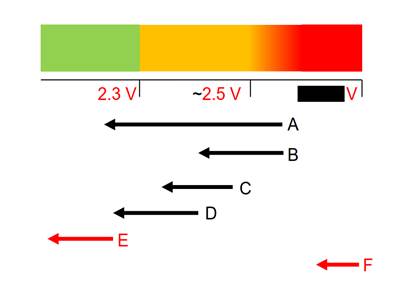
- Any distinction between the two arguments blurred somewhat when the point of construction was applied to one of the issues on infringement - whether Intel's accused voltage regulators contained protection circuitry. The voltage limits were solely within the knowledge of Intel. They are not published and were to begin with treated as confidential. Intel provided three figures. One was what was called the "punch-through" voltage, which would cause instantaneous destruction of the switching transistors. There was a lower figure, which I can identify as 2.5V - during the course of argument Intel helpfully agreed that it could be made public. Intel said that this was the relevant figure for assessing infringement because, based on real world conditions, this was the maximum voltage to which the transistors in their accused products could be exposed while maintaining a 5-year product lifetime reliability, Intel's target lifetime for such a test.
- There was also in argument a figure of 2.3V, which was presented by Intel to the German court hearing parallel proceedings as being the relevant figure. In this court Intel backed away from it, saying that it is an overly conservative figure.
- Intel had a pleading point. The parties were required by an Order of the court to file and serve Statements of Case on this point of construction. R2's Statement of Case said that the voltage spike protection circuitry must:
"... ensure that the voltage across the transistors does not exceed the maximum allowed voltage during the operation of the switched mode regulator circuitry."
- Intel agreed with this and no doubt it is correct. But the relevant voltage will depend on what the "maximum allowed voltage" is, as correctly identified. If Intel's implied case is that the maximum is whatever Intel say it is, I disagree.
- "Voltage spike protection circuitry" is not a term of art so I am not much assisted by the experts, save that they were agreed in the joint statement of the CGK that degradation of transistors can include:
"... the type of degradation that is most relevant to gradual accumulation of damage from stress on the transistor caused by persistent exposure to smaller over-voltages over a long period of time (which ultimately compromises the reliability of the transistor/renders it unable to be controlled effectively)."
- Paragraph [0065] of the Patent states that the added precautions discussed in later paragraphs, i.e. the voltage spike protection circuitry, are required to avoid "deleterious impact on the reliability of the converter [i.e. the voltage regulator of claim 1]". Paragraph [0070] says that ringing may "cause a loss in efficiency" of the voltage regulator.
- I take the view that voltage spike protection circuitry of the regulator must be suitable for protecting the switched mode regulator circuitry - the switching transistors - from voltage spikes and/or ringing which would cause a significant deleterious impact to the reliability and/or efficiency of the voltage regulator, whether instantaneously or over the course of the lifetime of the regulator that would have been contemplated by the skilled person at the priority date. The circuitry must be suitable for reducing such spikes and/or ringing to levels at which there will be no such impact.
- The foregoing assumes that the switching transistors would be exposed to spikes and/or ringing which would cause such impact in the absence of the voltage spike protection circuitry. It was agreed by the parties that if this were not the case, the candidate circuitry would not provide any meaningful protection and therefore would not qualify as protection circuitry.
- There is a nuance here. The Patent identifies consumer electronic devices, typically mobile phones, as products characteristic of those in which voltage regulators of the Patent would be used. I think I am entitled to assume that purchasers of mobile phones expect them to be appropriately reliable and that the skilled person would have believed this to be the case. This implies more than that the switching transistors of the voltage regulator are protected from voltages which are likely to cause a significant impact to the reliability and/or efficiency of the voltage regulator. A purchaser of a phone would not be satisfied with an assurance that on balance it is unlikely that the transistors will be damaged by voltage spikes. A purchaser would expect protection throughout the expected lifetime of the phone from spikes which could credibly cause such impact.
- R2 argued that it would be sufficient if the relevant circuitry increases the level of protection from voltage spikes within appropriate limits. Even if the circuitry does not have the effect of reducing spikes from levels which would cause maximum damage to levels would cause none but instead provides some lesser degree of protection from voltage spikes, the circuitry would still qualify as voltage spike protection circuitry within the meaning of claim 1. I agree, provided the degree of protection is significant, meaning more than insignificant.
Interleaved between
- Integer 1.5 of claim 1 requires that the charge-storage circuit segments be interleaved between the switching block segments. "Interleaved" is not a term of art in the context of the claim.
- "Interleaved" is a technical term of art in a different context, one that has application to these proceedings which I will discuss in due course. But as was clear to all, that is not the meaning intended in claim 1. Its meaning there, which I will call its non-technical meaning, is not self-evident, in fact odd.
- "Interleaved" would have an apparent non-technical meaning if one were discussing, say, the interleaving of two piles of sheets of paper. I would take it to require that the piles are brought together such that the surfaces of sheets in the first pile are in contact with the surfaces of sheets in the second pile. It may result in substantial alternation between sheets from the first and second piles. Shuffling playing cards could achieve a similar interleaving effect.
- In the context of charge-storage circuit segments and switching block segments on a chip, this sort of interleaving would make no sense and neither party suggested that the word would be interpreted in that way by the skilled person.
- Another difficulty is that "interleaved" does not appear anywhere in the description, so there is no direct assistance from that source.
- R2 argued that the term must be approached purposively. As explained in the Patent and confirmed by the experts, parasitic inductance increases with the length of connecting wires. Therefore to minimise it, the charge-storage circuit segments and the switching block segments should be placed as close to each other on the chip as is possible. "Interleaved" simply means arranging for the two types of segment to be in physically close proximity.
- Although interleaved is not a term of art, I think the experts' instinctive reaction to the term is of some relevance. R2's expert, Professor Alarcón, said in his first report:
"374. ... The Skilled Person would have understood that term to refer to arrangements in which the charge storage circuit segments are physically arranged in close proximity to corresponding switching block segments (as discussed in [0077]–[0080] and depicted in Figures 20-22 of the Patent) ..."
- For Intel, Professor Nauta's thoughts were consistent with this, although he preferred not to be pinned down: In his first report he said:
"107. From my reading of the Patent overall I understand that the core concepts the authors are seeking to present as inventive are:
...
b. the subdivision of switching circuitry and spike protection circuitry (respectively) into smaller segments or blocks, arranged proximally to one another in a certain physical arrangement (referred to in the claims of the Patent as 'interleaving') to minimise parasitic inductance from the associated connections; ..."
- Thus, Professor Nauta's impression was that the meaning of "interleaved" was to be derived from the purpose stated in the Patent of minimising parasitic inductance from the connections between the switching circuitry and spike protections circuitry, i.e. to keep them as short as possible. This was to be achieved by what Professor Nauta called "a certain physical arrangement", though he was undecided as to what that arrangement was, save that it must fulfil the purpose just mentioned. Later in his report he said expressly that he was not clear what "interleaved" means.
- In argument Intel distanced themselves from their expert's lack of commitment on this point and submitted that "interleaved" means that the charge-storage circuits must be located between the switching blocks, as shown in Figure 21 (see above). In that diagram there is a repeated arrangement of charge-storage circuit segments positioned on each side of the switching blocks. Intel supported this contention with seven reasons.
- First, it fits the natural meaning of "interleaved between". Secondly, "between" must be given meaning. Thirdly, the Patent's paragraph [0078] provides a guide:
"In an embodiment, the protection circuitry is further subdivided such that a portion of the protection circuit is disposed on each side of the switching circuit segment, and optionally in other convenient locations proximate to the switches themselves."
- In that sentence, Intel argued, the embodiment of claim 1 is described in the first part, which the sentence differentiates from the separate and non-claimed embodiment in which the protection circuitry is merely proximate to the switching circuit segments in other convenient locations.
- Fourthly, when the Patent meant "proximate" it said so. Claim 1 could have used that word but instead opted for "interleaved", which does not mean the same thing. Fifthly, this is what is shown in Figures 21 and 22 of the Patent. Sixthly, Professor Alarcón had confirmed in cross-examination that "near" or "proximate" permits longer connections than having charge-storage segments each side of the switching blocks.
- Finally, Intel contended that at the priority date it was part of the CGK that the capacitors and transistors could be divided into segments and placed in close proximity across the chip, "spread all over like a fabric" to use the words of Professor Nauta. The skilled person would assume that "interleaved" means something more.
- I accept that the purpose of "interleaved" is as both experts understood. The purpose is to minimise the length of the connections between the segments. The question is whether "interleaved between" would have been taken by the skilled person to imply something more specific.
- I agree that the sentence in paragraph [0078] is a statement of the embodiment which in the end was claimed as the invention. But I think it is artificial to split the sentence in two as Intel prefers. To my mind it simply explains that the subdivided segments of the protection circuitry can be disposed on each side of a switching segment or, at the implementer's option, other convenient locations provided they are proximate to the switching segment to which they are connected.
- In my view the skilled person would see no reason why the implementer of the invention should be limited to having the charge-storage circuits located between the switching blocks. It is true that the patentee could have said "in close proximity" in claim 1 if that was the intended meaning, but equally the claim could have specified that the charge-storage circuits must be between the switching blocks but chose not to. Figures 21 and 22, which show the latter arrangement, are stated to be examples of the invention, nothing more.
- It is also true that the arrangement gives a more obvious meaning to "between", but the term in issue is "interleaved between" and it hardly no more fits that arrangement than having the charge-storage circuitry scattered between the switching blocks in no strictly fixed pattern.
- I do not read the cross-examination of Professor Alarcón on this topic, on which Intel relies, as a concession that putting the charge-storing circuits always between two switching blocks is bound to result in minimising the length of the connections between them and that by extension "interleaved between" must require such an arrangement. As R2 pointed out, that cannot be right because such an arrangement encompasses having switching segments on each side of capacitor segments but distanced from them. The point that Professor Alarcón made plain was that the length of the connections should be minimised but there will also be other design considerations - it is always a trade-off.
- The skilled person would puzzle over the meaning of "interleaved between" in claim 1 but in my view would conclude that it is a purposive requirement, that the charge-storage circuit segments and switching block segments which are associated should be placed close to each other to minimise to the extent possible the length of the connections, always having in mind other design considerations. This will inevitably have some design impact: the charge-storage circuit segments and the switching block segments will be interleaved, in the intended sense, by virtue of their arrangement in closely associated pairs or groups, as opposed to the charge-storage circuits and switching blocks each being siloed together. But there is no more detailed stipulation about their respective positions. Anything more would have been seen to impose an unacceptable straightjacket on the design, overriding other design requirements which may be important.
Single phase only or multiphase possible
- Claim 1 is not expressly limited to a regulator which operates only in a single phase. All the examples in the Patent are so limited, but that of itself establishes nothing. In Supponor Limited v AIM Sport Development AG [2024] EWCA Civ 396, Birss LJ, with whom Phillips and Males LJJ agreed, said:
"[39] ... Supponor's argument is an example of a familiar wrong approach to the construction of patent claims. Limitations which are not present in the claim language are not to be read in by reference to examples which appear in the specification. The skilled person reading a patent understands that the examples are simply that. If the claim language is broad - as the term 'image property' clearly is - then the claim is correspondingly broad, for good or ill. The fact that the result will be that the claim therefore covers other approaches, different from those in the examples, is not on its own a reason to read the claim in a limited way. In some cases the consequences of different possible constructions e.g. for validity, might be relevant but only if those consequences would be part of the skilled person's thinking based on the patent and the common general knowledge."
- R2 argued that because claim 1 requires that the switching block segments are connected, they must have the same connected output inductor. In consequence, the inductor can only operate in a single phase.
- In his report, Professor Alarcón said that the Patent is clear that the switching block segments are connected to a common inductor, rather than separate output inductors which is the way in which multiphase buck converters were typically implemented at the priority date. If he meant that no other arrangement is shown in the examples, I agree. If he meant that the Patent contained a clear stipulation to this effect, no unambiguous direction was identified. His use of the word "typically" suggests that multiphase converters may not always be connected to a single output inductor.
- R2 quoted a passage from the cross-examination of Professor Nauta. He had been discussing the teaching in the description of the Patent and had agreed that there was nothing in that teaching which hinted at anything other than a single phase with a single output inductor. He accepted that Figure 21 has switching block elements connected in parallel with a single output. Still referring to that Figure, there followed a passage quoted in R2's closing:
"Q. Because the outputs are operating in parallel, we know that the switches must operate synchronously so that all the top switches open and close on the same timing and all of the bottom switches open and close on the same timing; yes?
A. Yes, if it a Phase I inductor, it has to be.
Q. Although it is not shown, the skilled person would know that the gate drive signals for all of the top switches must be connected in parallel and the same for all of the bottom switches; yes?
A. Yes, the gate's signals can be connected or you have a driver for each slice, but they are synchronously switched."
- R2 sought to rely on this to show that the invention claimed has switching block elements connected in parallel with a single output and so must therefore be confined to single phase operation. I disagree. Professor Nauta was just talking about the arrangement shown in Figure 21.
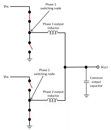
- I accept R2's point that if the system has a single output inductor it can only operate in a single phase. But it is not self-evident to me that because the switching block elements of claim 1 must be connected, perforce there is only one output inductor and one phase. The parties' agreed Statement of CGK included this diagram of a two-phase buck converter, omitting the control circuitry and feedback loop:

- The diagram shows two output inductors. The diagram has a legend which starts "A two-phase buck converter." Intel pointed out that although the switches are shown to be operating out of phase, they are connected, which is all that claim 1 requires, and shown to have a single output. R2 argued that "connected" means that the switching block elements must have the same connected control signals at the gates, the same connected output to the output inductor and the same connected supply rails. I was not directed by R2 to any wording in the Patent which imports these requirements into the simple word "connected". In support R2 just referred to Professor Nauta's evidence in relation to Figure 21 already discussed above.
- I agree with Intel that on a straightforward reading of the words of claim 1, the switching block elements shown in the above diagram are connected. I am not persuaded that the skilled person would interpret claim 1 to be more restricted in terms of phase than the words of the claim themselves suggest. I find that the voltage regulator of claim 1 could operate in a single phase or in multi-phase, notwithstanding that the switches must be connected.
Sun
- Sun is a paper entitled "3D Power Delivery for Microprocessors and High-Performance ASICs" (an ASIC is an application-specific integrated circuit) by Jian Sun and others of the Rensselaer Polytechnic Institute, New York. It was presented at a conference in Anaheim, California in 2007.
- In the introduction Sun states that conventionally power is delivered to microprocessors and ASICs using a voltage regulator mounted on the motherboard, i.e. outside the chip. This results in a long interconnect between the regulator and processor, leading to parasitic inductance and consequent current instability. It requires large numbers of decoupling capacitors located along the power delivery path, causes expensive use of board area around the processor to accommodate power pins and imposes a difficulty in delivering multiple supply voltages.
- The paper proposes what it calls a fundamentally different approach to power delivery. The principal innovation, as the title of the paper implies, is the use of three-dimensional (3D) architecture in the integration of the power supply in the processor. The voltage regulator becomes an integral part of the chip, but it is mounted above the processor wafer as opposed to being part of a flat 2D arrangement. Professor Nauta described the authors as a leading research group primarily interested in 3D integration.
- Sun discusses the difficulties inherent in a 3D design and continues:
"To determine the feasibility and performance of such monolithic dc-dc converters for 3D power delivery, we developed a fully integrated, two-phase interleaved buck converter with linear feedback control in a 180 nm SiGe BiCMOS process. The converter operates at around 200 MHz switching frequency, ..."
- Monolithic means that the voltage converter is located on the chip. An SiGe BiCMOS process is an advanced type of CMOS arrangement made from silicon and germanium. The Sun buck converter operated at the high level of switching frequency contemplated by the Patent.
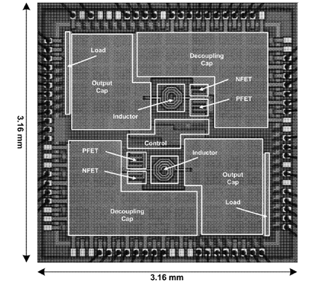
- Sun provides an illustration of the prototype chip developed:

- There are two "cells", top and bottom, each with output and decoupling capacitors largely surrounding an inductor and the switches. The latter are marked NFET and PFET, i.e. field effect transistors, in fact pairs of CMOS transistors, being respectively the low side and high side switches. (The letters N and P prefixing the FETs denote different charge carriers; the distinction is immaterial here). The control circuitry is in the centre of the chip. The capacitors, transistors and inductors of each cell make up an on-chip voltage regulator which, taken together, form a two-phase buck converter.
- Sun notes that the capacitors take up most of the area, 57.9% of it. The decoupling capacitors are needed to filter the discontinuous input current, limiting voltage spikes due to the parasitic inductance between the chip and the input voltage source outside the chip.
- Sun states:
"Input capacitors are needed to filter out the discontinuous input current so as to limit the di/dt voltage generated through the parasitic inductance between the input voltage source and the prototype chip."
- The term "di/dt voltage" comes from the well-established relationship between the voltage (V) across an inductor and the rate of change of the current (di/dt) in amps per second passing through the inductor having inductance L (in Henrys):
V = L x di/dt
- Thus, the greater the rate of change of current, the higher the voltage spike across the inductor, parasitic or otherwise.
- Professor Alarcón explained that the opening and closing of the high side PFET switches causes a discontinuous input current. When this discontinuous current passes through the line connecting the input voltage source and the chip, which will have parasitic inductance, it generates voltage spikes causing the current fluctuations. These need filtering. Professor Nauta agreed.
- There is a graph in Sun which shows the measured efficiency of the converter under different switching frequencies and local conditions. The authors state that a maximum efficiency of 64% is achieved at 200 MHz with an output current of 500 mA.
- The filtering required is reduced by operating the two cells 180o out of phase, exploiting the advantage of interleaving - in the technical sense foreshadowed above, not the claim 1 sense. Sun says:
"Interleaving is known to cancel the output ripple current in multiphase buck converters; an unexploited benefit of interleaving is that it also reduces input current ripple of multiphase buck converters."
- Professor Alarcón said that the ripple in the output current is fundamentally different to ripple in the input current. He described the idea of reducing the latter as "an intriguing observation."
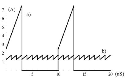
- The authors of Sun explain and develop the idea of using interleaving for the input current by proposing the use of 12 cells. In a thought experiment they compare the input current ripple where all 12 cells are synchronized with the ripple where the 12 cells are operated in an interleaved manner. They present a graph to compare the theoretical ripples of 10 synchronized parallel cells (shown as (a)) with those of 10 interleaved cells (b):

- The X axis is time in nanoseconds, the Y axis is the input current in amps. Sun says:
"The combination of small ripple amplitude and much higher ripple frequency implies that the input filter capacitance required by 10 interleaved converter cells can actually be smaller than that required by a single cell."
- The authors draw the following conclusions from their work on the prototype and their thoughts on how it may be improved:
"3D power delivery overcomes the limitations of conventional 2D power delivery architecture by eliminating most of the interconnect parasitics. Fully monolithic dc-dc converters compatible with the 3D platform are capable of meeting the needs of future microprocessors and high-performance ASICs for multiple, dynamically scalable, sub-1V supply voltages. The 3D platform can tolerate less efficient voltage regulators, and can be utilized to achieve more efficient converter design. The proposed cellular converter architecture enables full utilization of the benefits of interleaving to reduce filtering requirements, and is ideally suited for 3D integration."
Novelty over Sun
- The law was not in dispute. I will quote a well-known passage from the judgment of Sachs LJ in General Tire & Rubber Co v Firestone Tyre & Rubber Co Ltd [1972] RPC 457, at 463 (approved by the House of Lords in Synthon BV v SmithKline Beecham plc [2005] UKHL 59, at [22]):
"If the prior inventor's publication contains a clear description of, or clear instructions to do or make, something that would infringe the patentee's claim is carried out after the grant of the patentee's patent, the patentee's claim will have been shown to lack the necessary novelty, that is to say, it will have been anticipated. The prior inventor, however, and the patentee may have approached the same device from different starting points and may for this reason, or it may be for other reasons, have so described their devices that it cannot be immediately discerned from a reading of the language which they have respectively used that they have discovered in truth the same device; but if carrying out the directions contained in the prior inventor's publication will inevitably result in something being made or done which, if the patentee's patent were valid, would constitute an infringement of the patentee's claim, this circumstance demonstrates that the patentee's claim has in fact been anticipated.
If, on the other hand, the prior publication contains a direction which is capable of being carried out in a manner which would infringe the patentee's claim, but would be at least as likely to be carried out in a way which would not do so, the patentee's claim will not have been anticipated, although it may fail on the ground of obviousness. To anticipate the patentee's claim the prior publication must contain clear and unmistakable directions to do what the patentee claims to have invented: Flour Oxidizing Co. Ltd. v. Carr & Co. Ltd. (1908) 25 R.P.C. 428 at 457, line 34, approved in B.T.H. Co. Ltd. v. Metropolitan Vickers Electrical Co. Ltd. (1928) 45 R.P.C. 1 at 24, line 1). A signpost, however clear, upon the road to the patentee's invention will not suffice. The prior inventor must be clearly shown to have planted his flag at the precise destination before the patentees."
- R2 argued that the following matters in claim 1 of the Patent are missing from Sun:
(1) Voltage spike protection circuitry (integer 1.2). There is no discussion of voltage spikes or reason to believe that there is any protection from voltage spikes.
(2) A dissipative element (integer 1.2).
(3) Connected switching block segments (integer 1.4).
(4) Switching elements subdivided into switching block segments (integer 1.4).
(5) Charge-storage circuit segments interleaved between switching block segments (integer 1.5).
- Argument was overwhelmingly directed to the first of these. I will take it last.
- It was not in dispute that a dissipative element is a component of the circuitry which dissipates energy or that a resistor does exactly this, dissipating energy in the form of heat. It follows that if there is resistance in the relevant circuitry, there will be a dissipative element. If there is voltage spike protection circuitry in Sun it takes the form of input decoupling capacitors. Professor Nauta said that those capacitors will have an equivalent series resistance, i.e. an internal resistance that appears in series with the capacitance of the device, which constitutes a dissipative element. Professor Alarcón accepted in cross-examination that this was correct.
- Moving to the next matter, Intel said that the switching elements - the transistors - in Sun are subdivided into connected switching block segments, as appears from Figure 9 (shown above). The transistors, shown as NFET and PFET, are subdivided into two switching block segments or sets, the sets being connected in parallel. One set is shown towards the top right and the other towards the bottom left. Each set is for one of the two phases. Professor Nauta supported this view in his first report.
- R2's argument depended on their construction of claim 1, specifically that part of their interpretation which would limit the claim to a regulator operating in a single phase. This, R2 said, flowed from the requirement that the switching block segments are connected. I have found that they may be connected in parallel, in which case the regulator could have multi-phase operation. I further find that the switching block elements in Sun described above are connected within the meaning of integer 1.4.
- With regard to the matter numbered (4) above, Professor Nauta said that the switching elements in Sun, the transistors, are subdivided into switching block segments, each segment for one phase.
- Professor Alarcón took the view that this was not the sort of subdivision contemplated in the Patent. The Patent is only concerned with subdividing the switches into segments such that each carries only a portion of the total output of the current of a single output inductor, with the regulator operating in one phase only.
- I have found that claim 1 is not limited to a regulator operating in one phase or that there must be only one output inductor. Integer 1.4 of claim 1 goes no further than requiring the switching elements to be divided into connected segments. I do not think that "subdivided" would have been understood to add anything over "divided" here. The transistors of Sun are divided and I have found that they are connected. Matter (4) is present in Sun.
- Turning to "interleaving", the presence of matter (5) in Sun depends on the construction of that term. Neither the two charge-storage circuit segments of Sun, the input decoupling capacitors, nor the two switching block segments, the two sets of transistors, are located together. They are apart, with the capacitors in each case partially surrounding and in close proximity with transistors. That satisfies the requirement of interleaving as I have found it to be.
- As earlier mentioned, the real point of dispute between the parties was whether Sun discloses voltage spike protection circuitry.
- Sun says nothing at all about voltage spike protection. It was not in dispute that the decoupling capacitors of Sun are there to decouple the input of the chip from that part downstream of the capacitor, to prevent electrical energy from being transferred to the downstream parts of the chip. They are shown to be arranged across the series and shunt switching elements of the input. Should there be voltages spikes they will, to some unidentified degree, reduce those spikes. The simple point made by R2 was that there is no way of knowing that they serve to protect the transistors from voltage spikes.
- For convenience, I repeat here my finding on the meaning of "voltage spike protection circuitry": the circuitry must be suitable for reducing the voltage spikes and/or ringing likely to occur at the input of the regulator to a level at which they will have no adverse impact. Adverse impact would be a significant deleterious effect on the reliability and/or efficiency of the voltage regulator, whether instantaneously or over the course of the lifetime of the regulator that would have been contemplated by the skilled person at the priority date.
- Professor Nauta explained that the chip in Sun is designed in 0.18 micron CMOS technology, adding that the Patent shows that transistors in this technology are designed to handle a maximum voltage of 1.8 volts. The Sun chip has an input voltage of 1.8 volts, so if there was a spike much higher "the chip would die". Relying on the type of connections used by the Sun chip, which Professor Nauta said were associated with high parasitic inductance (the details of the connection type and its properties do not matter), the professor stated
"I know the chip works so there has to be spike protection, otherwise it would not work. It is as simple as that."
- R2 pointed out that Sun does not identify the maximum allowable voltage of its transistors and criticised Professor Nauta for drawing inferences about that from the Patent. They said that there was no reason to suppose that the reader of Sun would believe that it was concerned with ringing or voltage spikes, or for that matter the reliability of the prototype disclosed. The prototype was not at that stage of development.
- Both sides relied on the cross-examination of Professor Nauta, where he was discussing the distinction between the sort of voltage spike that would instantly incapacitate the transistor from the lower level of voltage spikes that would degrade a transistor over time:
"A. ... The degradation to sudden death is a very small voltage difference, it goes really bad at some point, so you do not want to be in the slow degradation part that is already bad.
Q. This degradation, we are talking long-term degradation, we are talking years of operation, not hours or weeks or months?
A. It could be ten years, high temperature.
Q. Given Sun is a prototype, there is no reason to think that it had undergone product reliability, testing, is there?
A. I do not think they did reliability testing, but they did measurements on the chip and it least it worked for a day, I would say. You cannot be close to this breakdown limit, you will really kill your transistors. The difference is tens of millivolts. It is quite, from slow degradation to death, it is a small step."
- R2 was correct regarding inferences to be drawn about the maximum permitted voltage for the transistors in Sun. Professor Nauta could not, or at least did not, refer to any document available at the priority date which would have assisted the skilled person in finding out the relevant voltage and which the skilled person would have consulted. Obviously, the content of the Patent was not available.
- Certainly, the skilled person would have known that the testing of the Sun chip that was done did not instantaneously destroy entirely the functioning of the transistors. As Professor Nauta put it, at least the chip worked for a day so it can be assumed that no spikes occurred over that day high enough to result in that sort of damage. However, the skilled person would have known nothing about the likely voltage limit of the transistors, how cautious or otherwise the Sun team was with the input voltage, the expected lifespan of the transistors or anything about the possibility of long term damage.
- In my judgment Sun does not contain clear and unmistakable directions to make a voltage regulator comprising voltage spike protection circuitry within the meaning of claim 1 of the Patent. Claim 1 does not lack novelty over Sun.
Inventive step over Sun
- There was no dispute about the law.
- Given my finding on novelty, the issue on inventive step is whether, having carefully read Sun, the skilled person at the priority date would have considered a variation on the Sun design to ensure that the circuitry of the regulator protects the transistors from voltage spikes. There was no issue regarding the skilled person's ability to achieve this with a reasonable expectation of success, so I can assume that if this would have been within the contemplation of the uninventive skilled person, claim 1 of the Patent lacks inventive step.
- Sun discusses the idea of scaling up the design to have several buck converter cells in parallel rather than just two (ten are proposed in Figure 13) thereby further dividing the input current between them and having each operate in a different phase so that their output currents could be interleaved (in the technical sense). If implemented, it would have served as a means of protecting against voltage spikes and ringing. Professor Nauta developed that idea in some detail, including the possibility of more than ten parallel cells. This proved to be an interesting blind alley. In their opening skeleton argument Intel disclaimed reliance on a scale up of Sun along these lines and I think they were right to do so.
- R2 argued that the skilled person would not have appreciated the problem of voltage spikes and ringing created by very high frequency converters. Sun does not discuss the high-efficiency fast switching which, as the Patent explains, gives rise to spikes and ringing. Absent that appreciation, R2 continued, there would have been no motive to consider protection circuitry. Professor Alarcón said (in his first report):
"367. I do not think the Skilled Person would have appreciated the issue of spiking and ringing for very high frequency converters at the priority date. However, once they were aware of the issue from the teaching of the Patent they would have considered that the spike protection circuitry proposed by the Patent was an effective solution to the problem."
- R2 had a second point: the skilled person would not have known that a dissipative element - electrical resistance - would be needed to dampen the effect of ringing, so introducing such an element would not have been obvious either. This is from Professor Alarcón's first report:
"370. Another noteworthy observation that the Skilled Person would also have taken from the Patent is that a dissipative element is needed in the spike protection circuitry for it to be effective. In the ordinary design of the power path for a voltage regulator at the priority date a designer would have sought to minimise the ESR [equivalent series resistance] of interconnects and other components as far as possible. The disclosure of the Patent runs counter to this - i.e. to either intentionally introduce resistive components or to leverage (and not seek to minimise as far as possible) the ESR associated with the capacitive element. The Patent teaches that this dissipative element is required in order to damp the identified high frequency ringing behaviour."
- Taking R2's second point first, the use of resistance in the regulator circuitry - in reality added resistance - to dampen ringing is referred to in the Patent but is not relevant to claim 1. Claim 1 requires the presence of a dissipative element, which is bound to be there to some degree, but does not require it to be suitable for achieving any particular result. The Sun design must have a dissipative element.
- R2's stronger point was about voltage spikes. Professor Nauta thought that the idea of adding voltage protection circuitry at the input was trivial. His evidence in his second report was that both (a) the problem of voltage spiking and ringing associated with rapid switching in very high frequency converters and (b) the need for resistance to dissipate such ringing were both part of the CGK. The potential for voltage spikes generated by rapid switching times is a necessary consequence of the very well-known relationship V = L x di/dt (discussed above). He said:
"80. In my view that Skilled Person would have been very well-aware of the potential issue of voltage spiking and ringing in high frequency switching circuits, including voltage converters. This would have been readily evident, not only: (a) as the simple consequence of absolute fundamentals of electrical engineering; but also (b) because this exact issue had been identified and addressed in other high frequency switching circuits such as the digital logic circuitry of processors (which, as I explained in paragraph 19 above, involved switching at frequencies up to and above 3 GHz by the year 2000); and (c) from discussions of this precise issue in textbooks and other literature in the field before the Priority Date."
- There were several documents with content which, as was agreed, reflected the CGK. That content contained warnings about the dangers of voltage spikes and the need for protection from them. Professor Alarcón said that these were always about systems in which the voltage regulator was off-chip, with decoupling capacitors at the power input. It was also part of his evidence that at the priority date the idea of having the regulator on-chip, though known, was not at all the standard arrangement, which may explain why there is nothing in the CGK documents about voltage protection if that arrangement is adopted. Also, Professor Alarcón did not give a reason why the skilled person would have thought that the need for protection could be discounted solely because the regulator was on-chip.
- Both experts were cross-examined at some length on the CGK documents and neither conceded during those cross-examinations that what he had said in his written evidence was incorrect regarding the skilled person's CGK in respect of the generation of voltage spikes and the need to protect transistors from them in the context of a system with an on-chip voltage regulator. If this were the only relevant evidence on the point, I would prefer that of Professor Nauta because his was based on the very well established equation V = L x di/dt and, separately, because Professor Alarcón did not explain why installing the voltage regulator on the chip would have been thought to make a difference to the danger from voltage spikes.
- However, Professor Alarcón was also cross-examined on this by reference to Sun:
"Q. ... Anyone making Sun and thinking about using Sun is going to know that the transistors they use will have a voltage limit?
A. Yes.
Q. They are not going to want to go over that?
A. Generally, no.
Q. Even if you were right, and we do not accept that, but even if you are right that Sun does not tell the reader about voltage-spike protection, it is something that the skilled person will have in mind and they will want to avoid voltage spikes on their transistors in the regulator?
A. In the very general sense, for of the specific field of on-chip power conversion, people were [not] very aware of this; not to say they were not.
Q. Let us take those people. Again, we do not accept that, but I understand you have this set of people who do not know that. They are going to test and very quickly find out, are they not, if they have voltage problems, because one tests either for immediate destruction or one tests for ----
A. Yes.
Q. You are going to do that, are you not?
A. Engineers of a team of a product will do that."
- Leaving aside the presence or absence of a "not", counsel's response to the third answer given by Professor Alarcón in that passage leaves some doubt about what he meant.
- On the other hand, Professor Alarcón agreed that a product like Sun would be tested for "voltage problems". The professor confirmed this shortly afterwards:
"Q. You are always going to have a reliability engineer who is going to check whether or not the transistors in your regulator are being harmed?
A. Yes, with -- yes, with the difference that these were new transistors, because they were very large. I am aware of the way engineers were stressing with test campaigns, large (indistinct) MOS off-chip in a standalone package, but I do not think there was enough experience to do so with very large transistors on a CMOS chip. But eventually, if this needs to go into a product, of course this needs to be done, of course."
- I think that whatever Professor Alarcón intended by the qualification in his final answer, he was saying that the skilled person would have known that if a product like the prototype in Sun was to be carried forward there would be tests to ensure that the transistors were not vulnerable to voltage problems. Professor Alarcón must have been well aware that the questions put were directed to the issue of voltage spikes, an important issue in the litigation on which he had been advising for many months. I therefore conclude that he had in mind tests to ensure that there was protection from voltage spikes.
- This suggests that the skilled person would have known at the priority date as a matter of generality that voltage spikes pose a danger to the transistors in a chip such as the one described in Sun. Whether he or she would have realised that the rapid switching times of the sort of transistors being used in the Sun prototype would have been a source of such voltage spikes does not matter in the end. Nor does it matter that the sort of testing discussed by Professor Alarcón would have happened some time down the road of product development. The important point is that the skilled person would have been aware that the Sun transistors might well be vulnerable to voltage spikes and that steps could be taken to protect the transistors.
- Even assuming the skilled person did not carry out tests to find out whether those steps would be needed, which is unlikely given what Professor Alarcón said, that did not make the adaptation any less obvious as an option.
- Claim 1 does not prescribe any particular means to achieve voltage protection. In his first report at paragraph 169 Professor Alarcón described a means well known in the CGK, namely by introducing a decoupling capacitor at the input of a voltage regulator.
- Professor Nauta commented on this evidence in his second report in a passage that was not challenged and which I accept as correct:
"86. I do not understand Professor Alarcón to be suggesting that - if he is wrong about the problem of voltage spiking and ringing in high frequency converters not being appreciated by the Skilled Person at the Priority Date - there is anything inventive about using decoupling capacitors per se to address that problem. Doing so is entirely consistent with and obvious from Professor Alarcón's own description of the function and purpose of decoupling capacitors in paragraph 169 and his explanation that a voltage regulator is required to maintain the output voltage within tolerated limits despite variations that occur at either the input or output ports (paragraphs 176 to 177)."
- Taking the evidence as a whole, in my view that skilled person at the priority date would have thought that an obvious optional variation on the design of the voltage regulator in Sun would have been to introduce voltage spike protection circuitry in the form of a decoupling capacitor at the input of the regulator circuitry. The skilled person would also have thought that protection was likely to be needed.
- Claim 1 lacks inventive step over Sun.
Proposed Amendments
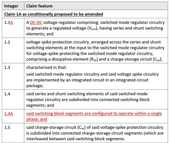
- There are the two proposed amendments to claim 1, identified as 1A and 1B. This is claim 1A separated into integers:

- There is nothing of significance in integer 1.1A. The agreed statement of CGK included this:
"'Voltage regulators' (also called 'power regulators') are a subset of power converters that convert one DC voltage to another DC voltage ..."
- The only other change to claim 1 as granted is to configure the switching block segments to operate in a single phase. In closing R2 did not resist Intel's submission that further varying the Sun design to have the transistors operate in a single phase would have been seen by the skilled person as another obvious change to make, along with introducing a decoupling capacitor to serve as protection against voltage spikes. Lest there be doubt, R2's expert, Professor Alarcón, said in cross-examination that having transistors operate in a single phase or in multiple phases would have been no more than a design consideration.
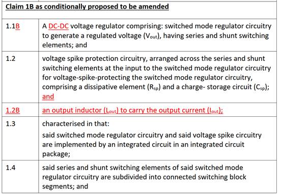
- This is claim 1B:


- The amendments in claim 1B are more extensive but I agree with Intel's submission that they can be collectively summarised as requiring the switching block segments to be connected in parallel and connected to a single output inductor and that this is another way of achieving the same result as claim 1A, namely that the switching block segments will then be bound to operate in a single phase. R2 did not submit otherwise.
- R2 did not press an argument that either claim 1A or claim 1B is inventive over Sun if claim 1 as granted is not. This was probably because it would have been inconsistent with their argument on infringement. R2 served a Statement of Case on Infringement dated 8 June 2023. At page 1 of the Annex there was a diagram of a FIVR. The annotation referred to the Intel FIVR disclosed in Intel's PPD which included this:
"A FIVR consists of multiple parallel phases, each with a single associated output inductor. Each such phase is a voltage regulator of the claim."
- R2's point there, for the purpose of arguing that Intel's FIVRs infringe, was that a multi-phase arrangement can be viewed as two or more single phase regulators operating in parallel. On that view, Sun discloses two single phase regulators operating in parallel.
- Speaking more generally, it was part of the CGK that voltage regulators were either single phase, the more orthodox arrangement, or multi-phase like Sun. It was also part of the CGK that if the switching block segments are connected to a single output inductor, the system will operate in single phase. This was put to Professor Alarcón, R2's expert, and he agreed. Discussing the alternatives of single phase and multi-phase, Professor Alarcón's evidence continued:
"Q. A skilled team is very well aware of both of those and which to use. Whether it is a single phase arrangement or a multi-phase arrangement, will be dependent on their design requirements and what they want, really?
A. In a general sense, yes. Time interleaving, power connected, multi-inductor, multi-phase were the natural option for off-chip voltage regulator models because there was the need to provide more current and, in turn, improve the design trade-offs of the output ripple. That was the state of the art.
Q. Right.
A. A design team would be aware of these things, which one to consider is not going to need a decision, but it is an engineering decision.
Q. Yes, and it is within the skill of our team to decide, it is a design consideration more than anything else, is it not?
A. It is a design consideration in general terms, yes."
- I take Professor Alarcón to have meant that the skilled person at the priority date would have known that single phase and multi-phase are obvious alternative options. The skilled person could always choose between them. Certainly, Sun speaks of the advantage of interleaving (in the technical sense), although only in the context of the elaborate thought experiment. The embodiment as constructed uses two-phase interleaving since its two cells are 180o out of phase. But as Professor Alarcón indicated, this was a design option. Simplifying it to one phase would have been seen by the skilled person as another option, even though it may lead to design trade-offs.
- I find that the variations on Sun contemplated by the skilled person would have included making it a single phase system by connecting the switching block elements to a single output inductor. No separate invention was alleged in respect of the other changes set out as the amendments of claim 1B, which are there only to cure any problem of added matter for claim 1A.
- Claim 1A and claim 1B both lack inventive step over Sun. It is not necessary for me to consider the issues raised by Intel regarding the allowability of the amendments due to added matter.
Infringement - the overall issues
- R2 alleges that Intel have infringed the Patent by marketing those of Intel's many devices which incorporate a fully integrated voltage regulator (FIVR), i.e. a voltage regulator that is located on the silicon chip. To make the proceedings manageable, it was agreed that infringement would be decided by reference to three representative Intel FIVRs.
- As discussed above, transistors have gates which alternate between on and off states, allowing current to flow or not flow. Each generation of transistors produced by a semiconductor manufacturer is known as a "technology node" or "process node". By convention each generation of technology node or process node was labelled according to the size of certain features of the transistor. The three representative Intel FIVRs are primarily distinguished by respectively corresponding to the 10nm, 14nm and 22nm process nodes.
- Intel argued that none of them falls within the claims of the Patent because each lacks two features of claim 1:
(1) Connected charge-storage segments which are interleaved between switching block segments (integer 1.5 as shown in the table of claim 1 above), and
(2) voltage spike protection circuitry for voltage spike protecting the switched mode regulator circuitry (integer 1.2).
- The first of these turns on whether the capacitors are interleaved between the transistors, which depends solely on the construction of the term "interleaved" as I have found it to be and the layout of the three FIVRs.
- The issue in relation to the second feature is, put at its simplest, whether the FIVRs are protected from voltage spikes. It was agreed for the purposes of these proceedings that infringement should be decided for all the FIVRs in issue by reference to Intel's 10nm FIVR.
Interleaved between
- I have found that the charge-storage circuit segments and switching block segments of claim 1 are interleaved if associated charge-storage segments and switching block segments are located close to each other to minimise to the extent possible the length of the connections, always having in mind other design considerations.
- It was common ground that on the foregoing construction all three of Intel's FIVRs satisfy this requirement.
Voltage spike protection circuitry
- My finding above in relation to voltage spike protection is that the circuitry of the regulator of claim 1 must be suitable for protecting the switched mode regulator circuitry - the switching transistors - from voltage spikes and/or ringing which would cause a significant deleterious impact to the reliability and/or efficiency of the voltage regulator, whether instantaneously or over the course of the lifetime of the regulator that would have been contemplated by the skilled person at the priority date.
- The parties were agreed that Intel's 10nm FIVR has MIM capacitors which will limit spikes in voltage at the FIVRs' current input. Whether the MIM capacitors qualify as voltage spike protection circuitry depends on (a) the relevant voltage threshold of the switching transistors in the FIVR, (b) the maximum voltage to which the transistors would be exposed in the absence of the capacitors and (c) the maximum voltage to which they are exposed with the capacitors in place in the normal way.
The relevant voltage threshold
- The voltage thresholds of Intel's FIVRs are not published. Intel created and applied their own models to find the threshold without input of any sort from R2. R2 were entirely reliant on the figure - as it turned out figures - supplied by Intel.
- Intel served a product and process description (PPD) in which it was stated:
"The maximum permitted peak transient voltage that can be experienced by the switching transistors whilst still achieving Intel's target level of reliability is approximately 2.5V."
- There was a footnote signalled after the word "reliability", which footnote read:
"Less than 300 defects per million over the 5-year product lifetime period for the 10nm Representative FIVR."
- The PPD went on to identify a higher voltage figure (still confidential). It stated:
"The specific maximum voltage limit that the switching transistors can be exposed before instantaneous destruction is observed is not known, but Intel testing results show that no instantaneous damage to the switching transistors of the 10 nm Representative FIVR was observed for Vccin input voltages up to at least [confidential figure in volts]"
- The PPD inferred from this that the voltage limit for instantaneous destruction was some value higher than the confidential figure given. It was of limited relevance and the parties were content to treat that figure as the voltage which would cause immediate destruction of the transistors.
- Parallel litigation is being conducted in Germany between Intel and R2 concerning the equivalent patent. The German court was told that the maximum permitted peak transient voltage for the relevant FIVRs is 2.3V. Apparently a court in Spain has been told by Intel that the correct figure is a range: 2.3-2.5V.
- Intel served a Response dated 25 October 2023 to a Request for Further Information from R2 about this. Intel said that they had at first applied a conservative assumption but had come to the view that the input voltage varied for different parts of the transistors. I will quote the next paragraph in full:
"The mode of degradation most relevant for a 5-year product lifetime reliability assessment for the switching transistors of the 10 nm Representative FIVR is time dependant dielectric breakdown ("TDDB") of the gate oxide of the NMOS transistors, as a result of the internal gate-drain voltage of the NMOS. With the conservative assumption noted above [footnote], a DC input voltage of 1.8 V (as specified in the PPD), and employing a reliability model for TDDB of the gate oxide of the NMOS transistor, the maximum permitted peak transient voltage to achieve the target reliability of less than [confidential figure] DPM over the 5-year product lifetime period for the 10 nm Representative FIVR is 2.3 V. Assuming a more real-world relationship between the total Vccin input voltage and the internal gate-drain voltage of the NMOS (likely to be in the region of 55%, according to Intel's analog transistor modelling) the maximum permitted peak transient voltage to achieve the target reliability of less than [confidential figure] DPM over the 5-year product lifetime period for the 10 nm Representative FIVR is approximately 2.5 V."
- The footnote reads:
"i.e. that 100% of the DC voltage and transient overshoot of the Vccin input voltage will be seen internally as a gate-drain voltage in the NMOS transistor."
- This indicates that although the 2.3V figure is based on conservative assumptions made by Intel, they are not absurdly conservative assumptions, as one might expect since the German court was told that it is the correct figure.
- It emerged during the evidence that Intel carried out experiments in the United States from which the 2.3 and 2.5V figures were derived. No Notice of Experiments was filed in this court (or anywhere else so far as I am aware) explaining Intel's methodology and the assumptions made in arriving at the two figures. R2 did not have the opportunity to comment on what was done and assumed, or to conduct their own repeats which may have shown that other figures are plausible, perhaps more plausible.
- Intel made two points about this. The first was that Dr Schaef signed the PPD and was not challenged on the ground that the 2.5V figure in the PPD was wrong.
- I am not sure what that cross-examination could have achieved aside from a pro-forma challenge without any material on which to base the challenge. Intel's Response to R2's Request for Further Information (see above) had given an explanation of the figures, 2.3 and 2.5V. R2 had to accept that explanation. The use of the 2.3V figure before the German court was not something about which Dr Schaef could be cross-examined. Professor Nauta was asked why the 2.3V figure was still being used in Germany and he stated his understanding that it was too late to change the figure there, but neither Professor Nauta nor Dr Schaef was a witness who could give authoritative evidence about what has been done by Intel in Germany and why, or in Spain for that matter.
- Secondly, Intel had a pleading point. Both sides conducted experiments to find the voltages which the 10 nm FIVR switching transistors are exposed to in use and to which they would be exposed without the MIM capacitors. In the usual way, R2's Notice of Experiments set out the facts R2 sought to prove and asked Intel to admit those facts. The Notice to Admit only referred to spikes above and below 2.5V. R2 never served a Notice asking Intel to admit that without the capacitors in place the transistors are exposed to spikes above 2.3V.
- Intel submitted that R2 had thereby pleaded reliance only on the 2.5V figure. That was the case that Intel had come to court to meet. Had R2 made it clear that it was now taking 2.3V to be the relevant voltage, Intel argued, they would have responded differently in reply, conducting further and more accurate experiments. Intel referred to this passage from the judgment of Birss J in Electromagnetic Geoservices ASA v Petroleum Geo-Services ASA [2016] EWHC 27 (Pat), at [21]:
"CPR PD63 7.1 requires that a party seeking to establish any fact by experimental proof conducted for the purpose of litigation must (my emphasis) serve a notice "(1) stating the facts which the party seeks to establish". This rule is vital for a number of reasons. It requires the party serving the notice to think precisely about what it is that the experiment is supposed to prove and what role it is to play in the case. It gives proper notice to the other party of what facts the experiment is supposed to prove. When the facts are properly set out it should also allow the court to understand what the experiment is for or at least should allow for that understanding to be arrived at fairly readily with further submissions. This in turn allows the court to retain control over the experimental evidence. The permission the court then gives to rely on the experimental evidence is permission to rely on it in order to prove those facts. If the party then changes its case and wishes to rely on the same experiment to prove something different, they may need permission to amend the Notice."
- The point which Birss J had in mind was the important function of the requirements to serve a notice stating the facts to be established by experiments, namely giving focus to the intended purpose of the experiments, giving proper notice the opposing side of that intended purpose and allowing the court to exercise informed control over the process. If there is a change to the facts to be proved, permission may be needed to amend the notice. Birss J was not considering the circumstances in which, if ever, a Notice of Experiments will limit the scope of the case which the serving party can run.
- I do not accept that a Notice to Admit associated with a Notice of Experiments will perforce limit a party's case in the way that a Statement of Case is liable to. It could be, for instance, that a fact unambiguously emerges from experiments which was not foreshadowed in the Notice to Admit but which is highly relevant to an issue before the court. It would make little sense for the court to ignore such a fact unless and until the Notice to Admit is amended.
- The real question raised by Intel is whether they were unfairly prevented from fully presenting their case on whether there is voltage spike protection in their 10nm FIVRs. In my view not. As appears from Intel's Response of October 2023, Intel were well aware by then if not before that the 2.3V figure would be in play at the trial. That is no doubt why Intel's expert gave evidence about it in his reports. There was time to conduct the more accurate experiments postulated by Intel in argument. Presumably Intel had in mind more accurate models to assess the damage threshold of their FIVRs, as before done without a Notice of Experiments and without the presence of any representative from R2. I must assume that instead of trying more accurate models Intel decided to keep their collective head down.
- Taking all this into account, I think that on balance Intel's conservative assumptions underlying the 2.3V figure are probably the most consistent with skilled person's expectation explained above: that there will be no credible risk of damage to the switching transistors over the expected lifetime of the FIVR.
- Accordingly, if Intel's 10nm FIVRs are exposed to spikes higher than 2.3V and the MIM capacitors reduce those spikes significantly to a level below 2.3V, the capacitors serve to protect the switched mode regulator circuitry from voltage spikes within the meaning of claim 1.
- R2 submitted that any reduction in spikes would constitute protection provided the figure without the MIM capacitors is above 2.3V and the figure with the capacitors is below 2.5V because the risk of damage would always then be reduced. R2 produced this diagram (I have redacted the voltage that would cause instantaneous damage):

- R2 submitted that any of the reductions in voltage spikes shown by the arrows marked A, B, C or D would qualify as protection. Those shown by arrows E and F would not. Subject to the reductions being significant, I accept that submission.
The experiments
- The voltage spikes to which Intel's 10nm FIVRs are exposed in use could not be directly measured. The parties had to develop models which provided a proxy as close as possible to the real thing and to conduct experiments based on those models. Instead of one agreed model, there were several. Each side strongly criticised the other's models.
- In January 2023 Intel sought and obtained an order for an expedited trial, but later backtracked and applied for an adjournment of the trial on the ground that they required further time for their experiments. The trial was adjourned but the delay did not unfortunately result in clarity.
- I acknowledge the high levels of expertise and effort which were devoted to the models on both sides. Still, the story of these experiments is not a shining example for all to follow.
The R2 Model
- R2 quite reasonably took on the task of finding evidence to establish infringement by making use of such information as it could access. Its approach was to reverse engineer parts of one of Intel's processors, a method known to those in the art as "tear-down". The physical configuration and material properties of the chip were analysed. R2 used this information and its own knowledge of how chips are made to re-construct the circuit of Intel's representative FIVR with values of inductance, resistance and capacitance for the components. This was called the Original R2 Model. R2 carried out experiments using this model to derive figures for the voltage spikes to which the transistors of the FIVR are exposed with and without the modifying effect of its MIM capacitors.
- The Original R2 Model and experiments of this type, or something very similar, were first deployed in the parallel German proceedings. So far as I am aware, they still are. For a while it seemed that the parties were agreed that this was as good a way as any to assess the relevant voltage spike figures. In fact, at the application by Intel for an expedited trial in January 2023 they submitted that little extra work had to be done in this regard before the trial in this court since the German R2 model was fit and ready for use in the English proceedings. Intel then had second thoughts.
- R2 served a Notice of Experiments on 19 May 2023. Intel responded on 2 June 2023 refusing to admit that the Original R2 Model was an accurate representation of the circuitry of their 10nm FIVR. There was an application to the court on 20 June 2023. The court ordered that Intel should specify their reasons why the Original R2 Model was not an accurate representation and also that Intel should disclose documents which would allow the court to reach a decision at trial on the accuracy of the model.
- On 7 July 2023 Intel applied to the court to adjourn the trial, saying that they needed time to properly critique the Original R2 Model and raising the possibility of creating their own variation on the model, filing extensive evidence as to why this was. The adjournment was granted but Intel were also required to file a Statement of Case setting out the precise changes to the Original R2 Model required, as they saw it, to allow the court to arrive at a conclusion at the trial as to the relevant reduction in voltage spikes. R2 was given the opportunity to file an Amended Notice of Experiments taking into account, if it so chose, the criticisms raised. Intel were given the opportunity to propose an amended model.
- Intel stated their criticisms of the R2 model. R2 made adjustments but complained that Intel had failed to provide enough information about Intel's FIVRs to make all amendments needed to meet Intel's criticisms. Intel said that to provide all the information R2 wanted was a task of disproportionate complexity.
- There was some force in Intel's position: R2 wanted a full circuit diagram of the entire FIVR with all parasitics extracted and included. Intel provided this information for a single block of transistors. It constituted over 9 million lines of code which as one might expect R2 was unable to digest and use. In fact R2 complained about it. However, it is not possible for me to reach a concluded view as to whether Intel could have found a simpler way to be more cooperative or whether R2 could have suggested one.
- The upshot was what has been called the "Amended R2 Model". This was still not agreed. Intel wanted five changes to be made to it. R2 said that they could not be done without further information from Intel. Intel provided some further information on the basis of which R2 made the fourth and fifth changes proposed, but not the first three. This resulted in the "Amended R2 Model with corrections 4 and 5". Like the parties, I will call them "corrections" and given the evidence about them, that is a fair term.
- Simulations were carried out by R2 on the Amended R2 Model and the Amended R2 Model with corrections 4 and 5, providing figures for voltages spikes with and without the effect of the MIM capacitors.
The ALTARM Model
- Meanwhile, Intel developed its own adaptation of the R2 Original Model. Professor Nauta was asked to perform simulations to determine the impact of Intel's five suggested corrections as opposed to just the last two. R2's model had been created using standard industry software called Cadence, a program used to simulate circuits. Professor Nauta preferred other standard software called LTSPICE and transposed the R2 Amended Model into that program. R2's expert, Dr Köse, made detailed criticisms of this transposition in his report and the consequent reliability of Professor Nauta's results.
- Professor Nauta accepted that his transposition would miss capacitances that should be present, so he adjusted the simulation. The result was referred to as the Adjusted LSPICE Transposed Amended R2 Model, or ALTARM for short. Next, Professor Nauta made five corrections to his ALTARM Model corresponding to the five corrections to the R2 Original Model proposed by Intel.
- Simulations were carried out on the ALTARM Model, again assessing voltage spikes with and without the MIM capacitors.
- Taking into account some of the criticisms of Dr Köse about his transposition, Professor Nauta made what he called a sensitivity analysis of his ALTARM model, adding a 40pH inductor. Only voltage spikes without the MIM capacitors were measured.
The Composite Model
- Professor Nauta had previously produced his own model which formed the subject of Intel's Amended Notice of Experiments. This was called the "Composite Model".
The models in issue
- These were the models referred to at the trial:
(1) The Amended R2 Model.
(2) The Amended R2 Model with corrections 4 and 5.
(3) The ALTARM Model with corrections 1-5.
(4) The ALTARM sensitivity analysis.
(5) The Composite Model.
- The voltage spike figures derived from these models are confined to a confidential annex to this judgment. For each model there was a figure for exposure with and without MIM capacitors, save for the ALTARM sensitivity analysis which only had the latter. They are stated with up to six decimal places, which implies an accuracy I find surprising. My impression, drawn from how they were derived, is that as reflections of the real voltage spikes in Intel's 10nm FIVRs they are a good deal more rough and ready than that.
- In fact R2's attitude towards the figures for the Amended R2 Model and that model with corrections 4 and 5 implies that R2 and its experts believe the voltages numbers to be more approximate than the decimal points suggest. R2's position was that corrections 4 and 5 make no significant difference. Before the trial R2 invited Intel to agree. Intel did not agree.
- If the numbers are indeed more approximate than they look, the experts did not state their views on the appropriate degree of approximation. I must take them as they are.
Intel's proposed corrections 1-3
- As I have said, Intel wanted five changes to the Original R2 Model, of which R2 made the fourth and fifth. I will consider the merits of the first three.
The mid-rail regulator switch
- The Intel voltage regulator, described in their PPD, has a connection between the high and low sides that passes through a switch called the mid-rail regulator. This is figure 1 of the PPD with the path highlighted in red:

- Intel's first criticism was that this connection and therefore the high and low side decoupling capacitance, labelled above, were absent from the Original R2 Model. It meant that their effect on the supply voltage and thus on the spikes had not been taken into account.
- Dr Köse, who made the R2 models, accepted that the absence of the connection largely eliminated the decoupling capacitance and that any remaining parasitic capacitance may be small. Dr Köse's reason for not implementing the connection in the R2 Amended Model was that Intel had not provided information about the parasitics associated with it. Dr Schaef for Intel said that the information could have been provided if he had been given enough resources to provide the information.
- Whether or not it was reasonable for Dr Köse to take the approach that he did, on the evidence the absence of the connection in the R2 Amended Model made a difference.
Modelling based on TSMC transistors
- The R2 Amended Model models transistors and decoupling capacitors using transistor models taken from the Taiwan Semiconductor Manufacturing Company (TSMC), not from Intel's transistors. That was because Intel did not supply the relevant information about their transistors. Professor Nauta accepted that it would have been helpful had Intel done so but added that this would not have accounted for associated parasitics.
- Intel's pleaded position, taken from their Statement of Case dated 21 February 2024, was this:
"25. It is correct the Defendants Intel has not proposed any 'corrections' to the sizing of the transistors used in the Amended R2 Model. The Defendants are not aware of TSMC's modelling processes and therefore cannot identify the 'corrections' to be made to the TSMC's modelling processes so that they materially reflect the transistor models used in the Amended R2 Model. It is correct that Intel has not provided its own transistor models for use in the Amended R2 Model - such proprietary 'process technology' information is of the highest sensitivity and confidentiality to Intel, and cannot be accessed or used outside of Intel's engineering compute environment, to which access cannot be granted externally, due to being an unacceptable security risk not only for Intel as a global leader in process and chip design, but as a matter of US national security.
26. The Defendants' position is that provision of Intel's own transistor models is not necessary in the circumstances. The Defendants are content for the Amended R2 Model to employ TSMC transistor models, or alternatively for ideal switches to be employed (as per the Revised Intel Model), in each case strictly provided that proper account is taken of the parasitic capacitance contributed by Intel's actual transistors (as determined by Intel from a layout extraction reflecting the parasitics from the switching transistors and power distribution grid to/from those transistors and provided to the Claimant in the Defendants' R2 Model Question Responses. The use of ideal switches in this respect is a 'conservative' or 'pessimistic' modelling assumption (i.e. an assumption adverse to the Defendants) in that the properties of ideal switches (which transition from open to closed and vice versa more rapidly than a real switch), are such that they will result in overestimation of the rate of change of current through the relevant parasitic inductances in the network and correspondingly the magnitude of voltage spikes at the input to the switching circuitry."
- In closing, Intel said that the relevant information was not available, which seems inconsistent with their pleaded case.
- According to their pleaded position, Intel had no difficulty with R2 using data taken from TMSC transistor models, provided that account was taken of parasitic capacitance. Intel provided a confidential figure for the combined capacitance associated with their transistors and power distribution grid. Professor Nauta carried out an estimate of the effective capacitance associated with the TMSC transistors, identifying a considerable difference between the two figures. Dr Köse said in cross-examination that Professor Nauta's estimate was based on a model with one capacitor and that this did not provide a reasonable approximation.
- Intel submitted that the four-terminal transistor model used by Dr Köse would underestimate the parasitic capacitance associated with the Intel transistors. I think it is fair to say that Dr Köse accepted that view in cross-examination.
The package parasitics
- What is sometimes called the "package model" of a circuit inevitably has "package parasitics", being parasitic resistance, capacitance and inductance.
- Intel provided confidential figures for the parasitic inductance and the parasitic resistance. As with the figure for the capacitance associated with the Intel transistors, Intel invited R2 to take these figures on trust, although they were verified by Dr Schaef in evidence. Dr Köse derived his own values by reverse engineering the Intel FIVR, providing figures which were very different from Intel's. Professor Nauta accepted that reverse engineering was a way to derive the figures, but said that Dr Köse had not done it correctly. In cross-examination Dr Köse said that Intel's approach in arriving at its figures was fundamentally wrong and he seemed to have no confidence in the accuracy of either his or Intel's values.
The status of the Amended R2 Model
- In closing R2 accepted that the Amended R2 Model, even with corrections 4 and 5, was not completely satisfactory and in an ideal world the first three corrections proposed by Intel would have been made. R2's argument was that it should have been put into a position to derive all the information necessary to create an accurate model and was prevented from doing so by Intel's failure to provide that information. As it was, and as Professor Nauta acknowledged, Dr Köse did his best with the information he had. On that basis, the Amended R2 Model should be accepted as an accurate model.
- Intel argued that the evidence established that the Amended R2 Model is inaccurate. Dr Köse could and should have implemented all five of Intel's corrections.
- I do not accept R2's contention that the Amended R2 Model, with or without corrections 4 and 5, should be assumed to be accurate just because Intel failed to provide R2 with information. It seems to me to be clear on the evidence that it is not accurate and that the voltage spikes measured using this model, both with and without MIM capacitors, are likely to be higher than those experienced in Intel's 10nm FIVRs. Beyond that, it is very difficult to say to what extent are they too high.
The status of Intel's ALTARM Model with corrections 1-5
- Intel argued that Professor Nauta's transposition of the R2 Model from Cadence software to LTSPICE (a variant of SPICE software) made no difference to the accuracy of the voltage spikes derived from the model, this time with all five of Intel's corrections made and that Dr Köse conceded this in cross-examination. That is not how I read Dr Köse's evidence. He maintained his position that the ALTARM Model was an inaccurate model of the Intel FIVR. It was put to him that there was no basis for the criticism; he could have done the transposition to LTSPICE himself and presented his own figures. Dr Köse accepted that he could have done that if he had had the data from Intel to implement all five corrections but it does not follow that the model was accurate.
- Professor Nauta was taken at length through Dr Köse's criticisms of the transposition from Cadence to LTSPICE. He did not change his expressed view that it made no material difference despite simplifications he had adopted in the process. In closing R2 highlighted just one criticism. Professor Nauta had been asked to compare graphs showing time domain waveforms derived in the experiments. These were graphs showing voltages using (a) the R2 Model before corrections and without the MIM capacitors and (b) the same thing transposed into LTSPICE. The maximum voltage spikes shown, the frequency of oscillation and the decay envelope are all significantly different. It was put to Professor Nauta that even before the five corrections were made, comparing the transposed model with R2's Cadence model was not comparing "apples with apples". Professor Nauta agreed, but explained the difference by saying that his model was conservative and R2's model was wrong.
Discussion
- The contradictory evidence of Professor Nauta and Dr Köse was in each case in part founded not on facts or reasoning the merits of which I can assess, but just on alternative assertions.
- However, I have found that the R2 Amended Model with corrections 4 and 5 is probably not an accurate representation of Intel's FIVR. Intel submitted that the ALTARM Model with all corrections is the best model available. That is a low bar, but I agree.
- Professor Nauta said that his ALTARM Model with all corrections was conservative. This was undermined to some limited extent by what was called a "sensitivity analysis" done by Professor Nauta to cross-check the figure for spikes without the MIM capacitors. A single parasitic component was introduced in place of the parasitics said to be created by the mid-rail circuitry. The figure for voltage spikes was significantly higher than that derived from the ALTARM model.
- In closing Intel's argument went no higher than saying that their Composite Model provides corroboration for their ALTARM Model with all corrections.
- R2 had several strongly argued criticisms about the Composite Model. Given Intel's position, I will comment on just two of them. A likely significant factor which accounts for differences in values between this model and the ALTARM model came from an adjustment made by Professor Nauta to the capacitance in the Composite Model. It emerged in cross-examination that the scale of the adjustment was based on a figure given to Professor Nauta by Intel, a figure which did not feature in any PPD produced by Intel and the derivation of which was nowhere explained. Even Professor Nauta could not justify it because he did not know where it came from. This was not a satisfactory way in which to create a model for litigation.
- The second point was curious for a different reason. In closing R2 drew my attention to this paragraph in Intel's second further amended PPD:
"The general tolerances between these simulations and the real world (i.e. difference between nominal parameters 'pre-silicon' and 'post-silicon' actual characteristics) is in the range of +/- 30%. This is due to variation in component values, package and board manufacturing tolerances, etc as part of the fabrication process."
- Responding to this in closing, Intel's counsel said that the product tolerance of + 30% applied to all models. If there were any doubt before, this seems to reinforce the perception that presenting the voltage spike figures (recorded in the Confidential Annex) to two or more decimal places is a nonsense.
- It may also imply that to ensure a satisfactory product tolerance in Intel's 10nm FIVRs as sold, I should add 30% to the voltage spike figures. But this was not a point taken up by either side.
Conclusion on infringement
- For the reasons stated, I will rely on the voltage spike figures derived from Intel's ALTARM Model with corrections 1-5 as the best guide I have to the spikes to which Intel's 10nm FIVRs are exposed, with and without the MIM capacitors. Taking those figures as they are, as did the parties' arguments at the trial, i.e. not rounding them up or down, the MIM capacitors provide modest protection. The voltage spikes to which the FIVR would be exposed without the MIM capacitors would not cause instant transistor damage. But over the course of five years' use, it is credible, to put the risk at its lowest, that the spikes and associated ringing would have a deleterious impact to the reliability and/or efficiency of the voltage regulator. The protection afforded by the MIM capacitors is modest but significant. Intel's 10nm FIVRs fall within claim 1 of the Patent. It follows that all the accused Intel FIVRs do.
Conclusion
- The Patent is invalid for lack of inventive step over Sun. Had it been valid, it would have been infringed.


